
Comply with the electronic products are light, multi-functional, integration, the development trend of PCB for high precision, high integration and lightweight direction, with a handheld, portable electronic products size shrinking, the requirements for printed circuit board as electronics carrier of fine is also increase year by year, high-end HDI products in mobile phones, digital products, communications networks, automotive electronic products field, such as demand rising in the number, the communication network and mobile phones for largest applications, especially in the market.
High-end HDI due to its characteristics of high integration, high density interconnect, which can effectively reduce wiring space, suitable for electronic products are lightweight, high transport requirements, from simple interconnection devices has become an important device in the product design and will gradually become the mainstream of consumer electronics with PCB, its output value proportion is increasing.
With the increase of customer groups, the diversification of product demand has gradually increased, and the demand for HDI PCB boards has grown rapidly with the existing customer groups and clients in development. Currently, the production capacity and product structure of HDI boards of simple HDI PCB stack up and second HDI PCB stack up have been increasing. Can not meet the future needs of the client, product structure adjustment is imminent, therefore, it is necessary to immediately implement the “high-precision board” project, start planning and production of more complex stack up HDI PCB, Anylayer, MSAP and other products to meet customer demand for high-end HDI board product market.
The most widely used HDI application and the highest output value are still the mobile phone boards, and the mainstream has been developed by 2+N+2, 3+N+3, towards the overall design of Anylayer.
The main board design of NB and handheld device HDI has been increasing year by year, and the HDI penetration rate is expected to reach more than 50% after 2020.
1.Consumer Driven Technology
The via-in-pad process supports more technology on fewer layers, proving that bigger is not always better. HDI PCB Technology is the leading reason for these transformations. Products do more, weigh less and are physically smaller. Specialty equipment, mini-components and thinner materials have allowed for electronics to shrink in size while expanding technology, quality and speed etc.
2.Key HDI Benefits
As consumer demands change, so must technology. By using HDI technology, designers now have the option to place more components on both sides of the raw PCB.Multiple via processes, including via in pad and blind via technology, allow designers more PCB real estate to place components that are smaller even closer together.
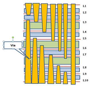
3.Via in Pad Process
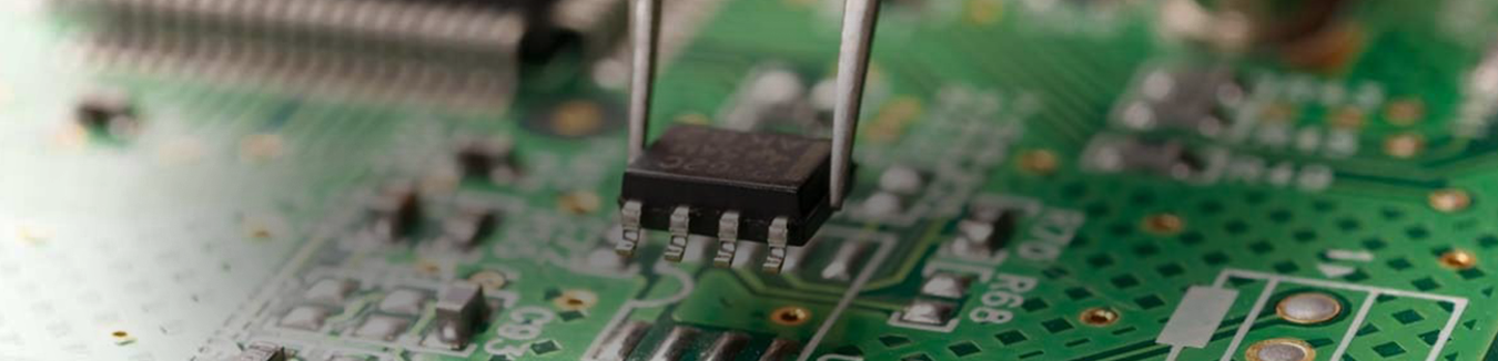
The via in pad process allows for vias to be placed within the surface of the flat lands. The via is plated and filled with either conductive or non-conductive epoxy then capped and plated over, making it virtually invisible.Sounds simple but there is an average of eight additional steps to complete this unique process. Specialty equipment and trained technicians follow the process closely to achieve the perfect hidden via.
4.Cost Effective HDI
While some consumer products shrink in size, quality remains the most important factor for the consumer second to price. Using HDI technology during design, it is possible to reduce an 8 layer through-hole PCB to a 4 layer HDI micro-via technology packed PCB. The wiring capabilities of a well-designed HDI 4 layer PCB can achieve the same or better functions as that of a standard 8 layer PCB.
5.Building Non-Conventional HDI Boards
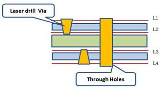
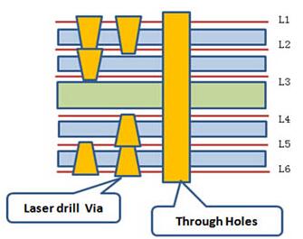
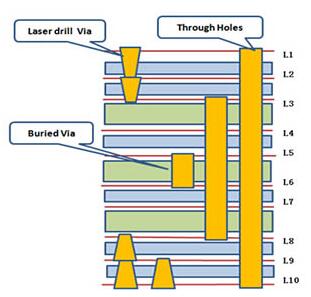
Successful manufacturing of HDI PCBs requires special equipment and processes such as laser drills, plugging, laser direct imaging and sequential lamination cycles. HDI boards have thinner lines, tighter spacing and tighter annular ring, and use thinner specialty materials. In order to successfully produce this type of HDI board, it requires additional time and a significant investment in manufacturing processes and equipment.
6.Laser Drill Technology
Drilling the smallest of micro vias allows for more technology on the board’s surface.
7.Lamination & Materials For HDI Boards
Advanced multilayer technology allows for designers to sequentially add additional pairs of layers to form a multilayer PCB.Choosing the right dielectric material for a PCB is important no matter what application you’re working on, but the stakes are higher with High Density Interconnect (HDI) technologies.so that is most important for multilayer PCB to use good materials.
8.HDI PCB used in many industries, including:
Digitial (Cameras, Audio, Video)
Automotive (Engine Control Units, GPS, Dashboard Electronics)
Computers (Laptops, Tablets, Wearable Electronics, Internet of Things – IoT)
Communication (Mobile phones, Modules, Routers, Switches)
HDI PCB Boards, one of the fastest growing technologies in PCBs, are now available at KingSong Technology.Our changing culture will continue to drive HDI technology and KingSong will be here to continue to support our Customer needs.Find a quality HDI PCB Manufacturer and Supplier,welcome choose KingSong.