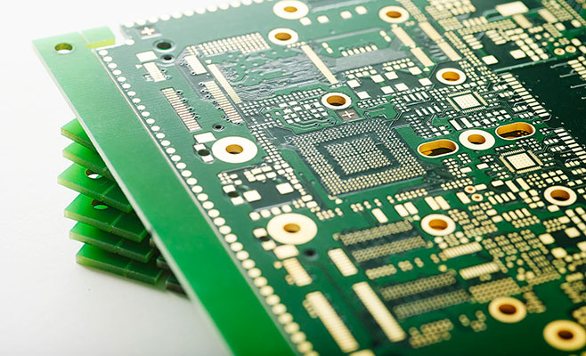
Blind & Buried vias PCB
Blind & Buried Vias PCB,PCB vias can be classified into through-hole via, blind via and buried via.When you want to put enough PTH vias on a circuit board but the space is limited, blind & buried vias PCB might be a solution.
Blind buried vias are used to connect between layers of PCB under restrictions of surface.
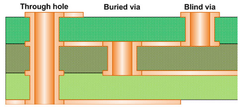
Blind via is a plated hole that connects only one outer layer to one or more inner layers. Buried via is a plated hole that connects two or more inner layers, but with no connection with the outer layer.
Benefit of blind & buried via
- Could meet the density constraints of wires and pads on a design without increasing the layer count or board size
- Reduce PCB circuit aspect ratio
Blind/buried vias PCB,also called HDI PCB meet the density improvement of boards without increase number of layers or board size. Therefore, blind/buried vias are usually applied in HDI PCBs. It frequently used in mobile phones, wireless commination, MID, Notebook etc.