
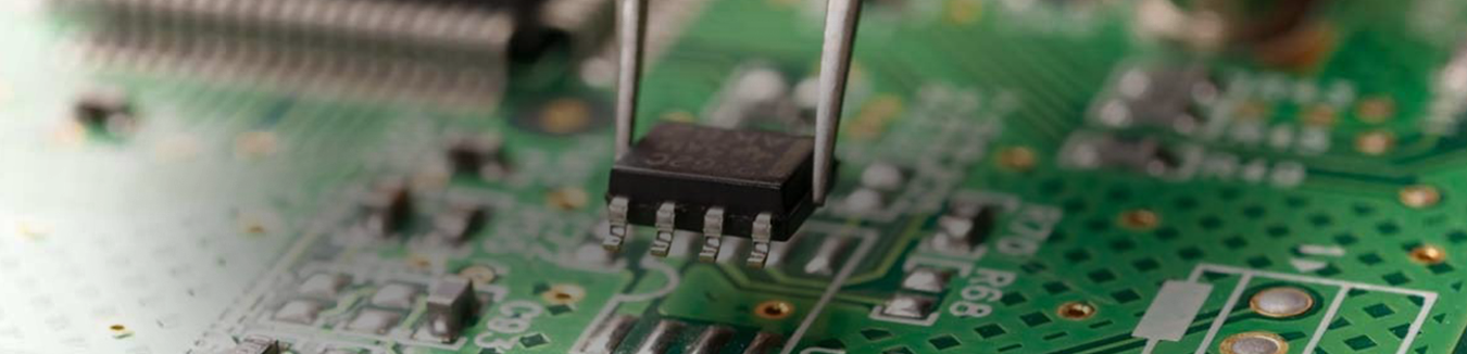
Everyone knows doing the principle diagram of the PCB is designed into a real piece of PCB, please don’t look down upon this process, there are a lot of things on the principle of practicable in engineering has difficult to achieve, or something that someone can achieve them,but others can not, so it is not difficult to make a PCB, but make a good PCB Prototype is not an easy thing.
Two major difficulties in the field of microelectronics is the high frequency signal and weak signal processing, PCB production level is particularly important in this respect, the same principle design, the same components, different people made PCB will have different results, so how to make a good PCB board?Based on our previous experience, we would like to discuss our views on the following aspects:
1. Define your goals
Received a design task, must first clear the design goals, is a Common PCB board, high-frequency PCB,small signal processing PCB or there are both high frequency and small signal processing of the PCB, if it is a common PCB, as long as do reasonable layout and tidy, mechanical size accurate, If the load line and long line,will be handled by a certain means, lighten the load,to strengthen the long line of the drive, the key is to prevent the long line’s reflection.When there are more than 40MHz signal lines on the board, special considerations are made for these signal lines, such as crosstalk.If frequency is higher, have more restrictions on the length of the wiring, according to the distribution parameters of network theory, the interaction between high speed circuit and its attachment is the decisive factor, the system can’t be ignored in design.With the improvement of the door transmission speed, on line against will increase, the crosstalk between adjacent signal lines will be proportional to the increase in, usually high-speed power consumption and heat dissipation of the circuit is very big, should cause enough attention when doing High Tg PCB.
When board have millivolt level even microvolt level when the weak signal, the signal will need special care, small signal is too weak, very vulnerable to other strong signal interference, shielding measures is often necessary, otherwise will greatly reduce the signal-to-noise ratio.So that useful signals are drowned out by noise and cannot be effectively extracted.
On board the measure also should be taken into consideration during the design phase, the physical location of test points, test point of isolation factors cannot be ignored, because some of the small signal and high frequency signal is not directly add probe to measure.
In addition, there are other related factors, such as the layer of boards, the package shape of the components and the mechanical strength of the boards.Before making PCB boards, you should have a design goal in mind.
2. Understand the requirements of the function of the components used in the layout
As we know, there are some special components in the layout have special requirements, such as LOTI and APH used analog signal amplifier, analog signal amplifier for power requirement for smooth, small ripple.The simulation of small signal parts should be kept away from power devices.On the OTI board, the small signal amplification part is also specially designed with a shielding mask to shield the stray electromagnetic interference.GLINK chips used in the NTOI board is the ECL process,power consumption big fever, to the problem of heat dissipation must be conducted when the layout must be special consideration, if the natural cooling, will put the GLINK chip in air flow is smooth, and out of the heat is not a big impact to other chips.If there is a horn or other high power device on board,it may also cause serious pollution of the power it should also pay enough attention.
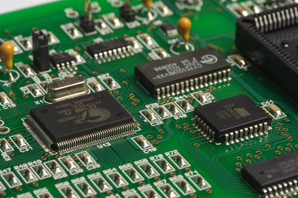
3. Consideration of component layout
The layout of the components first one factor to consider is the performance, closely related to the connection of components together as far as possible, especially for some high speed line, the layout is to make it as short as possible to separate power signal and small signal device.In the premise of meeting the performance of the circuit, it is also necessary to consider the arrangement of the components in order, beautiful, convenient to test, the mechanical size of the board, the position of the socket, etc.
The transmission delay time of grounding and interconnection in the high-speed system is also the first factor to be considered when designing the system.Signal on the transmission time had a great influence on the overall system speed, especially for high-speed ECL circuits, although high speed integrated circuit block itself, but as a result of on the floor with common interconnect (every 30 cm long, about the delay of the 2 ns) bring the increase of the delay time, can make the system speed is greatly reduced. Like a shift register, synchronous counter this synchronization working parts on the same piece of card, best because of the different transmission delay time of the clock signal on the board is not equal, could lead to a shift register produce errors, if not on a plate, where synchronization is the key, from public clock source connected to the clock line must be equal to the length of the board.
4. Consideration of wiring
With the design of OTNI and star optical fiber network, more than 100MHz of the high speed signal line will need to be designed in the future. Some basic concepts of high speed line will be introduced here.
Transmission line
Any “long” signaling pathway on a printed circuit board can be considered a transmission line.If the transmission delay of the line is much shorter than the signal rise time, the reflection of the owner during the signal rise will be submerged.No longer appear overshoot, recoil and ringing, for at the moment, most of the MOS circuit, because of the rise time of line transmission delay time is much bigger, so it can be in metres long and no signal distortion.And for faster logic circuits, especially ultra-high speed ECL.
In the case of integrated circuits, the length of the traces must be significantly shortened in order to maintain the integrity of the signal due to faster edge speeds.
There are two ways to make the high-speed circuit in a relatively long line work without serious distortion, is used for the rapid decline in edge TTL schottky diode clamping method, make impulse be restraint in a diode is lower than the ground potential pressure drop on the level of reducing the recoil at the back of the amplitude, the slower the rising edge of the overshoot is allowed, but it is level “H” in a state of relatively high output impedance of the circuit (50 ~ 80 Ω)attenuation.In addition, due to the level of “H” state immunity, larger recoil problem is not very outstanding, device of HCT series, if using schottky diode clamping and series resistance side connect the method, the improved effect will be more obvious.
When there is a fan out along the signal line, the TTL shaping method described above is lacking in the higher bit rate and faster edge speed.Because there are reflected waves in the line, they will tend to be synthesized at the high rate, thus causing serious distortion of the signal and decreasing anti-interference ability.Therefore, in order to solve the reflection problem, another method is usually used in the ECL system: line impedance matching method.In this way the reflection is controlled and the integrity of the signal is guaranteed.