Welcome to KingSong PCB Technology
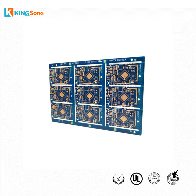
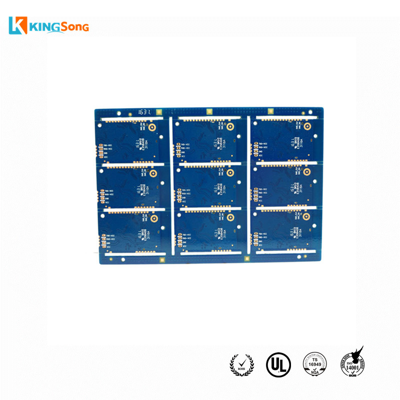
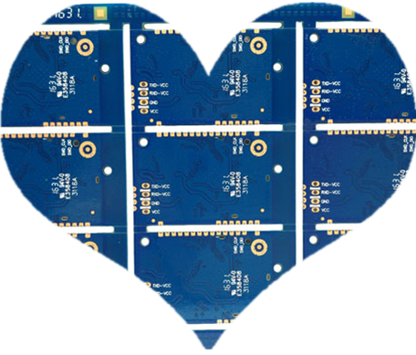
Image:Double-sided OSP Half Hole Circuit Board With Impedance Control
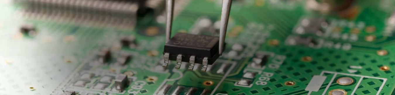
This 2 layer OSP PCB board used in Industrial Application,such as Electronic Tuner,Intelligent Controller products,A PCB Circuit Board With OSP Surface Finish is a coating between a component and a bare pcb board,Impedance Control and Half Holes Plated at the edge of the board will be the special and complex technology during the production process,but that is no any problem for us as professional PCB manufacturer,we are not only provide rigid pcb services,but also offer flexible pcb manufacturing & full assembled services.
1.Detail PCB Manufacturing Capabilities:
| No. |
Item |
Mass Production |
Prototype |
| 1 |
Layers |
1-8 Layers |
1-20 Layers |
| 2 |
Max. Panel Size |
600*770mm( 23.62″*30.31″) |
600*770mm(23.62″*30.31″) 500*1200mm(19.69″*47.24″) |
| 3 |
Max.Board Thickness |
8.5mm |
8.5mm |
| 4 |
Min. Board Thickness |
2L:0.3mm,
4L:0.4mm,
6L:0.8mm |
2L:0.2mm,
4L:0.4mm.
6L:0.6mm |
| 5 |
Min Inner Layer Clearance |
0.1mm(4mil) |
0.1mm(4mil) |
| 6 |
Min Line width |
0.1mm(4/4 mil) |
0.075mm(3/3 mil) |
| 7 |
Min Line space |
0.1mm(4/4 mil) |
0.075mm(3/3 mil) |
| 8 |
Min.Hole Size |
0.15mm(8mil) |
0.1mm(6mil) |
| 9 |
Min plated hole thickness |
20um(0.8mil) |
20um(0.8mil) |
| 10 |
Min Blind/Buried hole size |
0.2mm(8mil) |
0.2mm(1-8layers)(8mil) |
| 11 |
PTH Dia. Tolerance |
±0.076mm(±3mil) |
±0.076mm(±3mil) |
| 12 |
Non PTH Dia. Tolerance |
±0.05mm(±2mil) |
±0.05mm(±2mil) |
| 13 |
Hole Position Deviation |
±0.05mm(±2mil) |
±0.05mm(±2mil) |
| 14 |
Heavy Coppe |
4oz/140μm |
6oz/175μm |
| 15 |
Min S/M Pitch |
0.1mm (4mil) |
0.1mm (4mil) |
| 16 |
Soldermask colour |
Green,black,Blue,White,Yellow,Red |
Green,black,Blue,White,Yellow,Red |
| 17 |
Silkscreen colour |
White,Yellow,Red,Black |
White,Yellow,Red,Black |
| 18 |
Outline |
Routing,V-Groove, Beveling punch |
Routing,V-Groove, Beveling punch |
| 19 |
Outline Tolerance |
±0.15mm ±6mil |
±0.15mm (±6mil) |
| 20 |
Peelable mask |
Top,bottom,double sided |
Top,bottom,double sided |
| 21 |
Controlled Impedance |
+/- 10% |
+/- 7% |
| 22 |
Insulation Resistance |
1×10¹²Ω(Normal) |
1×10¹²Ω(Normal) |
| 23 |
Through Hole Resistance |
<300Ω(Normal) |
<300Ω(Normal) |
| 24 |
Thermal Shock |
3×10sec@288℃ |
3×10sec@288℃ |
| 25 |
Warp and Twist |
≤0.7% |
≤0.7% |
| 26 |
Electric Strength |
>1.3KV/mm |
>1.4KV/mm |
| 27 |
Peel Strength |
1.4N/mm |
1.4N/mm |
| 28 |
Solder Mask Abrasion |
>6H |
>6H |
| 29 |
Flammability |
94V-0 |
94V-0 |
| 30 |
Test Voltage |
50-330V |
50-330V |
2.PCB lead time:(if you need urgent service,we also can meet)
| Description |
Double Layer |
4 Layer |
6 Layer |
8 Layer |
10 Layer or above |
| Sample(WD) |
4 |
7 |
8 |
10 |
12 |
| Mass production(WD) |
7-9 |
10-12 |
13-15 |
16 |
20 |
3.Package:Inner vacuum packing,Outer standard carton box packing.
4.Shipping:
A:By DHL,UPS,Fedex,TNT etc.
B:By sea for mass quantity according to customer’s requirement.
5.If need quotation for your PCB projects,pls provide following info:
A:Quote quantity,
B:Gerber file in 274-x format,
C:Technical requirement or parameters(material,layer,copper thickness,
board thickness,surface finishing,solder mask/silkscreen color…)
If any inquiry or want to learn more,please send email to us freely or chat by online system,thanks for your support in advance!