

A planned life can make people feel comfortable.Naturally, the planned PCB design is also more convincing, and the layout engineer can be less detour.
The layer number of PCB board is generally not determined in advance, it is planned by the engineer’s comprehensive board, and the total number of layers consists of the number of signal layers and the number of layers of the power supply.
1. Planning of power supply and stratum number
The number of layers of power supply is mainly determined by the number of types of power supply, distribution, load capacity, performance index of single board and cost of single board.The setting of the power plane needs to satisfy two conditions: the power supply is not interlaced.Avoid important cross-section of adjacent layers.
The layer number setting of the ground should pay attention to the following points: the main devices should have a relatively complete ground plane in the face of the second layer;Important signals such as high speed, high frequency, clock, etc.Main power supply and ground plane tight coupling, reduce the power plane impedance and so on.
2. Signal layer number planning
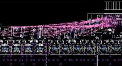
Wiring channels are usually important factors that determine the number of signal layers.It is important to know whether there is a deep BGA and connector on the board, and the depth of BGA and the PIN spacing of BGA are the key to determine the number of BGA line.For example, BGA of 1.0mm can cross two lines normally, 0.8mm BGA cross hole can only pass one line, and the number of line between the two lines is very different.The connector mainly considers its depth, which is a pair of differential lines between two holes.


Second, we must consider the wiring board high-speed signal channel,because when high-speed signal processing requirements of the conditions is more, need to consider a stub, line spacing, such factors as the reference plane, so you need to give priority to its wiring channel is enough.
Finally, the bottleneck area is planned. After the basic layout is processed, it is necessary to focus on the narrow bottleneck area.Considering the difference line, sensitive signal line, special signal topology, etc., how many lines can be calculated in the bottleneck area, and how many layers can be used to make all the necessary lines pass through this area.

Considering the above two points,basically not appear to go some parts of the line, some people say: pcb design is like a high-rise building building process, the layout of the wiring layer is one of the design drawings, planning well, the wiring naturally It can be done.
Before starting the PCB design,you should know PCB size:this depends on your product size,PCB layers:the more layers, the more complex the manufacturing of the PCB will be,The more layers the PCB has, the more costly it will be to manufacture it,KingSong PCB specilized in providing PCB manufacturing services . We could support diverse printed circuit board manufacturing service from single layer to 36 layers to meet your different PCB requirements.When you finish the layout design,you get a Gerber file,this file will be used by your PCB manufacturer,Even though there are many companies that provide these services,but we would like to recommend King-PCB.COM.