
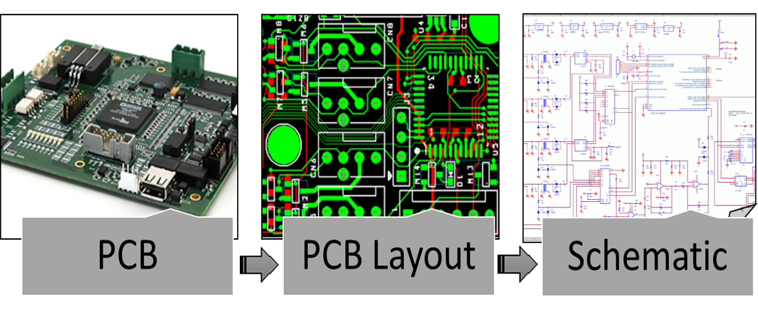
PCB copy,that is already in the premise of electronic products and circuit boards in kind,Using reverse engineering to reverse the circuit board analysis, the original products of PCB file, bom and schematic diagram, technical documents for 1:1 reduction operation, and then reuse these technical files and production of circuit boards and PCB board, components welding system debugging, complete the original circuit model of the whole copy.
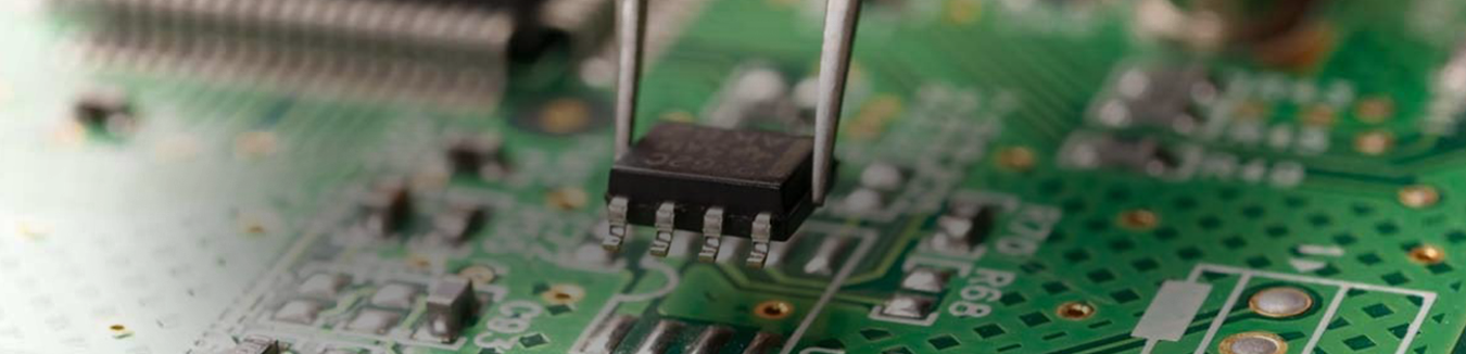
1. Take a piece of PCB. First, the model, parameters and position of all the components are recorded on the paper, especially in the direction of the diode and the tertiary tube, and the direction of the IC gap.That is better to use a digital camera to take two photos of components’ direction.
2. Remove all the components and remove the tin from the PAD hole.Use alcohol to scrub the boards clean, then put them in the scanner, and then scan the scanner slightly higher to get a clearer image of the board.Then re-use water yarn paper to the top and bottom slightly polished, polished to the copper film shiny, into the scanner, start PHOTOSHOP,and separate the two layers in color.Note that the PCB must be vertically aligned in the scanner, otherwise the scanned image cannot be used.
3, Adjust the contrast of the canvas, the contrast, make have part of the copper film and not part of the copper film contrast, then put the figure into black and white, check whether the line is clear, if not clear, will continue to adjust.If it is clear, save the image as BMP format two files. If you find the graphics problem, you need to modify it in PHOTOSHOP.
4, Will convert two BMP format into PROTEL format file, in PROTEL transfer into two layers, if the location of two layer PAD and VIA basic coincidence, suggests several steps before doing a good job, if there is deviation, repeat the third step, until the anastomosis,The TOP layer of BMP can be converted to PCB, be careful to into a SILK layer, the layer is yellow, then you are in the TOP layer is tracing, and drawing device according to the second step.Delete the SILK layer after the drawing, and repeat to know all the layers are drawn.
5. Transfer TOP.PCB and BOT PCB in PROTEL to a picture.Use a laser printer to print the TOP LAYER, BOTTOM LAYER to the transparent film (1:1 ratio), put the film on the PCB, compare the error, if yes, if successful.
Due to the electronic products are composed of all kinds of circuit board core control part of the work, therefore, the use of PCB copy board such a process to complete the complete set of technical information on any electronic product extraction and product imitation and cloning.