Welcome to KingSong PCB Technology
Image:FR4 4 Layers Impedance Control And HASL Surface Finishing PCB Prototype Fabrication
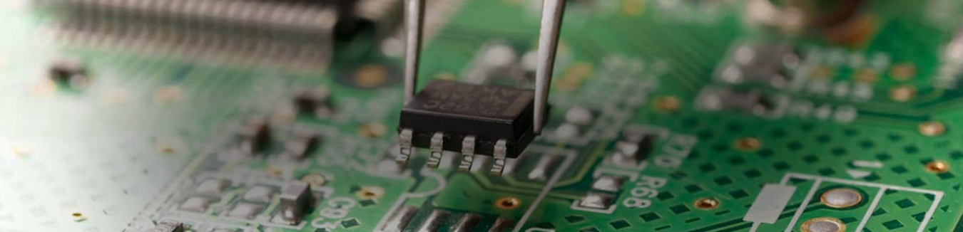
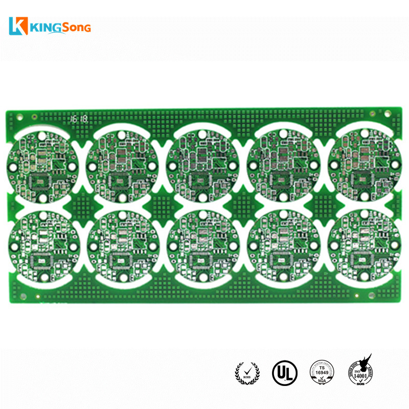
This Printed Circuit Board is a FR4 4 Layers Impedance Control And HASL Surface Finishing PCB Prototype Fabrication,used in Consumer Electronics,some like Camera of The Car Recorder,A PCB Circuit Board with HASL Surface Finishing is a coating between a component and a bare pcb circuit board,KingSong Tehnology as a professional PCB Manufacturer are not only offer 4 layers pcb board,but also 6 layer pcb, 8 layer pcb or 10 layer pcb etc.
1.Detail PCB Manufacturing Capabilities:
| No. |
Item |
Mass Production |
Prototype |
| 1 |
Layers |
1-8 Layers |
1-36 Layers |
| 2 |
Max. Panel Size |
600*770mm( 23.62″*30.31″) |
600*770mm(23.62″*30.31″) 500*1200mm(19.69″*47.24″) |
| 3 |
Max.Board Thickness |
8.5mm |
8.5mm |
| 4 |
Min. Board Thickness |
2L:0.3mm,
4L:0.4mm,
6L:0.8mm |
2L:0.2mm,
4L:0.4mm.
6L:0.6mm |
| 5 |
Min Inner Layer Clearance |
0.1mm(4mil) |
0.1mm(4mil) |
| 6 |
Min Line width |
0.075mm(3/3 mil) |
0.075mm(3/3 mil) |
| 7 |
Min Line space |
0.075mm(3/3 mil) |
0.075mm(3/3 mil) |
| 8 |
Min.Hole Size |
0.15mm(6mil) |
0.15mm(6mil) |
| 9 |
Min plated hole thickness |
20um(0.8mil) |
20um(0.8mil) |
| 10 |
Min Blind/Buried hole size |
0.1mm(4mil) |
0.1mm(1-8layers)(4mil) |
| 11 |
PTH Dia. Tolerance |
±0.076mm(±3mil) |
±0.076mm(±3mil) |
| 12 |
Non PTH Dia. Tolerance |
±0.05mm(±2mil) |
±0.05mm(±2mil) |
| 13 |
Hole Position Deviation |
±0.05mm(±2mil) |
±0.05mm(±2mil) |
| 14 |
Heavy Coppe |
4oz/140μm |
6oz/175μm |
| 15 |
Min S/M Pitch |
0.1mm (4mil) |
0.1mm (4mil) |
| 16 |
Soldermask colour |
Green,black,Blue,White,Yellow,Red |
Green,black,Blue,White,Yellow,Red |
| 17 |
Silkscreen colour |
White,Yellow,Red,Black |
White,Yellow,Red,Black |
| 18 |
Outline |
Routing,V-Groove, Beveling punch |
Routing,V-Groove, Beveling punch |
| 19 |
Outline Tolerance |
±0.15mm ±6mil |
±0.15mm (±6mil) |
| 20 |
Peelable mask |
Top,bottom,double sided |
Top,bottom,double sided |
| 21 |
Controlled Impedance |
+/- 10% |
+/- 7% |
| 22 |
Insulation Resistance |
1×10¹²Ω(Normal) |
1×10¹²Ω(Normal) |
| 23 |
Through Hole Resistance |
<300Ω(Normal) |
<300Ω(Normal) |
| 24 |
Thermal Shock |
3×10sec@288℃ |
3×10sec@288℃ |
| 25 |
Warp and Twist |
≤0.7% |
≤0.7% |
| 26 |
Electric Strength |
>1.3KV/mm |
>1.4KV/mm |
| 27 |
Peel Strength |
1.4N/mm |
1.4N/mm |
| 28 |
Solder Mask Abrasion |
>6H |
>6H |
| 29 |
Flammability |
94V-0 |
94V-0 |
| 30 |
Test Voltage |
50-330V |
50-330V |
2.PCB lead time:(if you need urgent service,we also can meet)
| Description |
Double Layer |
4 Layer |
6 Layer |
8 Layer |
10 Layer or above |
| Sample(WD) |
3-5 |
7 |
8 |
10 |
12 |
| Mass production(WD) |
7-9 |
10-12 |
13-15 |
16 |
20 |
3.Package:Inner vacuum packing,Outer standard carton box packing.
4.Shipping:
A:By DHL,UPS,Fedex,TNT etc.
B:By sea for mass quantity according to customer’s requirement.
5.If need quotation for your PCB projects,pls provide following info:
A:Quote quantity,
B:Gerber file in 274-x format,
C:Technical requirement or parameters(material,layer,copper thickness,
board thickness,surface finishing,solder mask/silkscreen color…)
If any inquiry or want to learn more,please send email to us freely or chat by online system,thanks for your support in advance!