
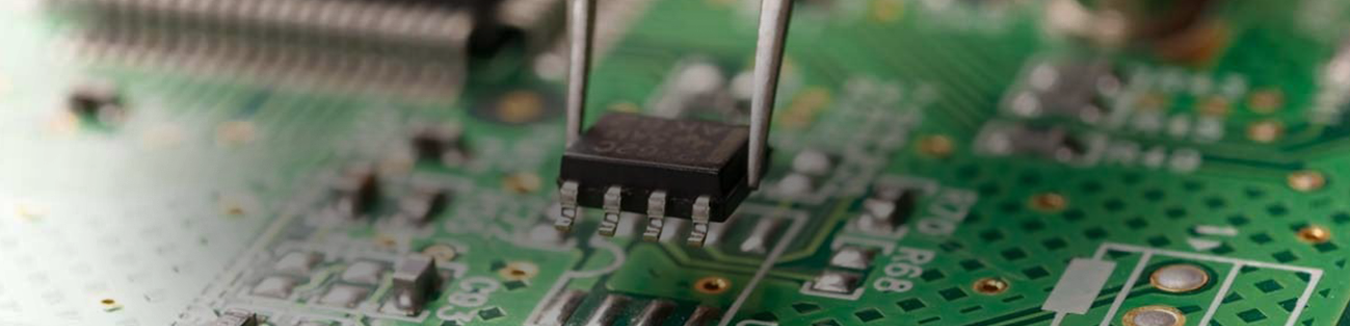
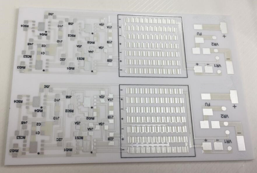
과학 기술의 발전과 함께, 인쇄 회로 기판필수적인 전자 부품되어 있으며, 인쇄 회로 기판은 Al2O3으로서 전자 substrate.Traditional 무기 기판으로 변경하고있다의 SiC, BeO를 그리고 AlN 기판의 열전도율이 물질 굽힘 강도 및 열팽창 계수는 현재 널리의 MCM substrate.The 연구의 산업 분야에서 사용되어, 양호한 성능을 갖는 세라믹 PCB 재료 의 저항 가열 소결 실리콘 카바이드를 사용하는 주원료로서 마이크론의 Al2O3 CaZrO3 등이며, 탐색 상대 밀도, 유전 상수 및 유전 손실 특성.
1.Relative 밀도 분석
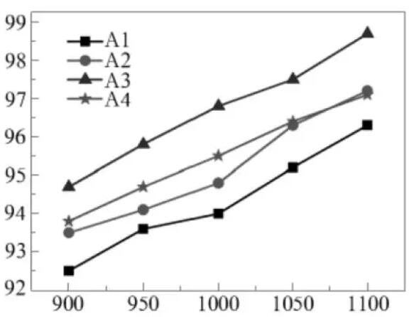
The influence of the relative density of alumina ceramic integrated circuit substrate with different micron Al2O3 and nano CaZrO3 powder was added.By a figure known as the temperature increases, the relative density with the increase of substrate material, temperature of 1100 ℃ maximum.When micron Al2O3 content is 60 wt %, the adding amount of nano ZrO2 is 10 wt %, the relative density of alumina ceramic pcb substrate integrated material relative to other formula is the largest, the sample is relatively dense, is beneficial to integration of alumina ceramics substrate material mechanics performance improvement.
2.Dielectric 일정한 분석
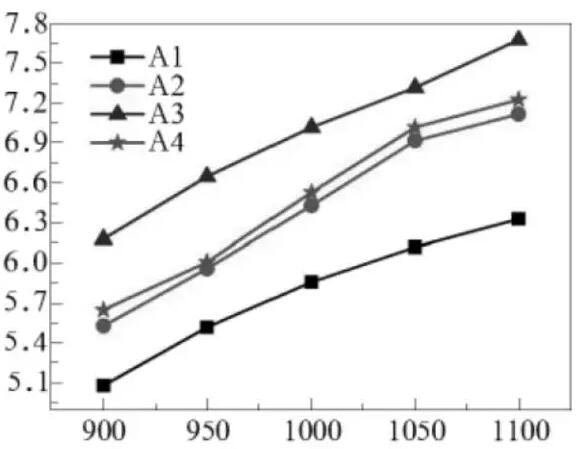
The above is the dielectric constant of the 세라믹 PCB는 material with the curve of sintering temperature.It can be seen that as the temperature rises, its dielectric constant increases.When the temperature reached 1100 ℃, the dielectric constant peak.When the addition of micron Al2O3 was changed from 50 wt% to 65 wt %, and the addition of nano-cazro3 was changed from 20 wt% to 5 wt %, the dielectric constant of the alumina integrated electric subgrade plate was first increased and then decreased.When the content of micron Al2O3 was 60 wt% and the content of nano CaZrO3 was 10 wt %, the sample performance was the best.This is because the factors that influence the dielectric constant are multifaceted, as long as the chemical composition of the formulation is involved, the more the alkali metal ion oxide content is, the greater the permittivity is.In addition, the thermal exercise of the ions and dipoles in the process of rising temperature increases, resulting in an increase in the permittivity.
3.Dielectric 손실 분석
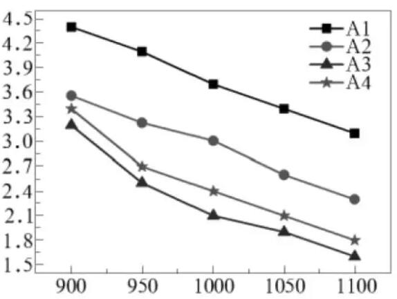
The above is the dielectric loss of the ceramic pcb cesubstrate material with the sintering temperature curve.As the temperature increases, the dielectric loss gradually decreases.When the micron Al2O3 in 50 wt % 65 wt % change between nano CaZrO3 between 20 wt % to 5 wt % change, dielectric loss reduced after increased first, when the micron Al2O3 content is 60 wt %, nano CaZrO3 amount to 10 wt %, and when the sintering temperature is 1100 ℃, the dielectric loss value of the minimum sample after sintering.
The dielectric loss of the ceramic pcb material is caused by the internal electron, ion drain and space charge polarization, and the smaller the volume resistivity of the material, the larger the dielectric loss.Of the existence of samples CaZrO3 Ca (superscript 2 +) ions of other low price and tetravalent Zr ions produce depressive effect, make the dielectric loss of samples increased, the Na2O and the existence of K2O, makes the ion K and Na ions as a result of the action of the double effect of alkali, make the network combined with close, so the sample dielectric loss less.